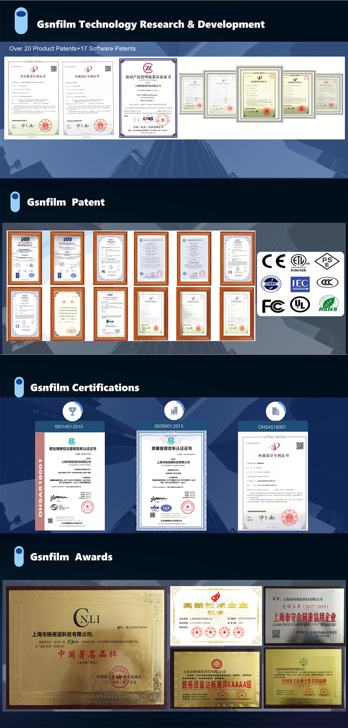
1. R & D and Innovation
GsnFilm has a professional R & D team composed of industry - leading experts and experienced engineers. They are constantly exploring and innovating in the field of dimming film technology. With years of in - depth research, we have mastered advanced liquid crystal - based dimming technologies, such as PDLC (Polymer - Dispersed Liquid Crystal) technology. This allows our dimming films to achieve fast - response light - control performance, quickly switching between transparent and opaque states with the application of an electric field. Our R & D center is equipped with state - of - the - art testing and experimental equipment, ensuring that every new product and technology can be fully tested and optimized before going to market.
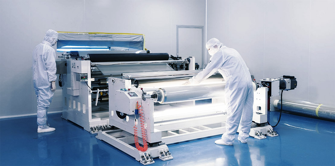
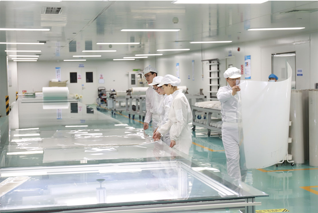
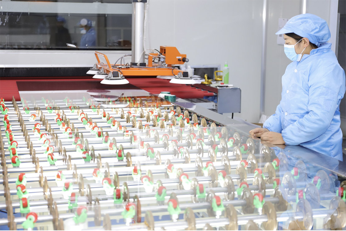
2. Production Capacity and Quality Control
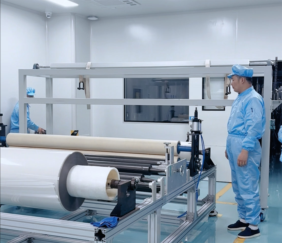
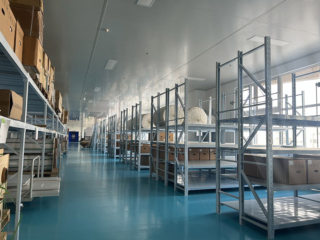
GsnFilm own a modern production base covering an area of 50,000 square meters, equipped with several advanced production lines. These production lines can produce high-quality dimming films with an annual output of 30+ millions square meters, meeting the growing market demands. From the selection of raw materials to the final product inspection, every step of the production process is strictly monitored.Gsnfilm use advanced manufacturing processes to ensure the stability and durability of our dimming films.
3. Product Range and Applications
GsnFilm product portfolio mainly includes standard dimming films, anti - UV dimming films, and high - temperature - resistant dimming films, etc. These products have a wide range of applications. In the architectural field, they are used in building facades, interior partitions, and glass doors and windows, which can not only adjust the indoor light environment but also enhance privacy protection and energy - saving performance. In the automotive industry, dimming films are applied to car sunroofs, side windows, etc., providing drivers and passengers with a more comfortable driving and riding experience by reducing glare and heat. In addition, they are also popular in the fields of commercial displays, exhibition halls, and high - end residential decoration.
4. Service and Customer Support
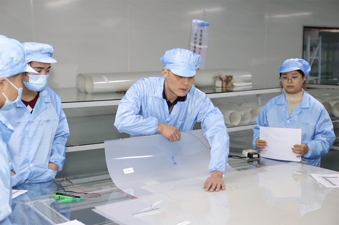
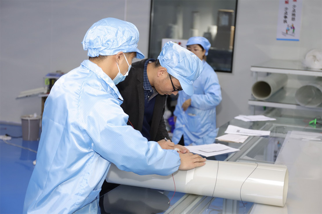
Customer satisfaction is gsnfilm’s top priority. We have a professional pre - sales team that can provide customers with detailed product information and professional technical advice, helping them choose the most suitable dimming film products according to their specific needs. Our after - sales service team is on standby 24/7 to solve any problems that customers may encounter during product installation and use. We also provide on - site installation guidance and training services to ensure that customers can use our products correctly and efficiently.
In the future, Gsnfilm will continue to uphold the spirit of innovation, improve product quality and service levels, and strive to become a world - class dimming film supplier, bringing more intelligent, energy - saving, and comfortable light - control solutions to the global market.
I. Strict selection of raw materials
A): PET & ITO Layer
Ultra-flat PET film:
Gsnfilm only uses imported optical-grade PET (Japan Toray, Japan Mitsubishi, Korea SKC), with a thickness tolerance of ±1%, surface roughness Ra≤0.1μm, and transmittance>87%~95%.
Nano-level conductive materials:
Indium tin oxide (ITO): Multilayer composite films (such as ITO+AZO+ITO) are plated by magnetron sputtering, with a square resistance of ≤15Ω/□, transmittance>88%, and anti-bending performance is improved by 3 times (can withstand 100,000 folding tests).
Alternatives: Nano silver wire (wire diameter <20nm) or single-walled carbon nanotube (SWCNT) conductive layer, suitable for flexible curved scenes, conductivity>10⁶ S/m.
B): High-end PDLC slurry
Liquid crystal material:
Gsnfilm Using chiral nematic liquid crystal or fluorinated liquid crystal (such as Merck E7 series improved type), the response speed is increased to ≤50ms, and the operating temperature range is extended to -40℃~85℃ (0℃~60℃ for ordinary products).
Polymer system:
Gsnfilm Using UV-curable acrylate prepolymer (such as Sartomer CN2200), adding nano-silicon dioxide (particle size 50nm, dispersion ≤5%) to enhance mechanical properties, glass transition temperature (Tg)>120℃.
Additive upgrade:
Adding light stabilizer (HALS) and antioxidant (hindered phenol), the UV resistance time is ≥5000 hours (about 2000 hours for ordinary products).
II. Ultra-precision coating and coating process
A): Vacuum magnetron sputtering coating
Multi-target co-sputtering:
In an environment with a vacuum degree of <10⁻³ Pa, ITO target and aluminum oxide (Al₂O₃) target are sputtered in sequence to form an ITO/Al₂O₃/ITO sandwich structure, which improves the scratch resistance of the conductive layer (hardness up to 4H).
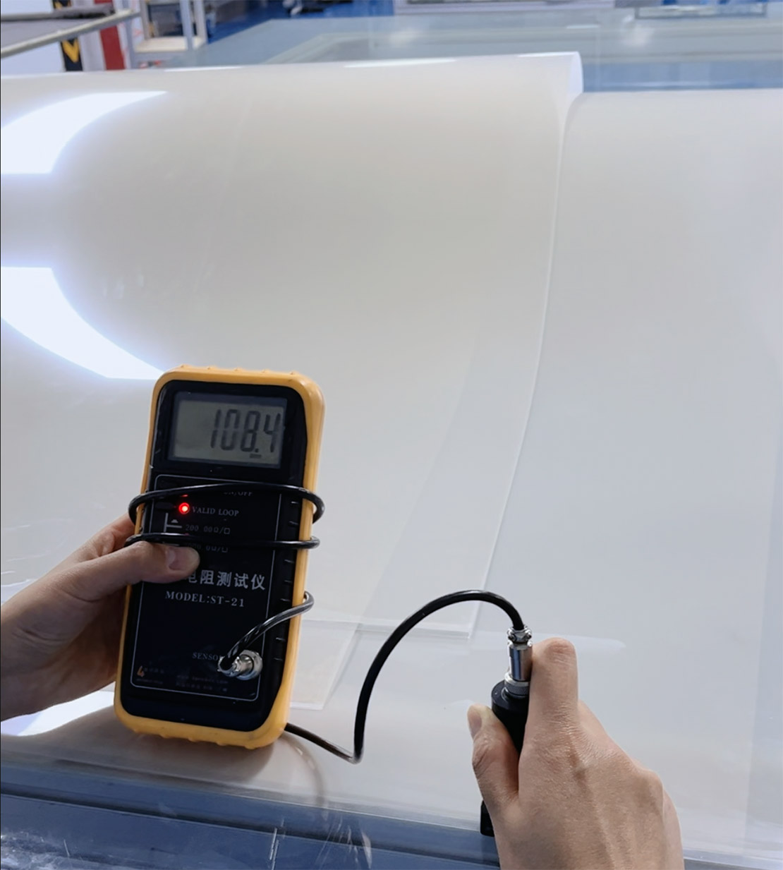
Online detection:
Equipped with a laser thickness gauge (accuracy ±1nm) and a four-probe tester (resolution 0.1Ω/□), real-time monitoring of film uniformity, local thickness deviation ≤2%.
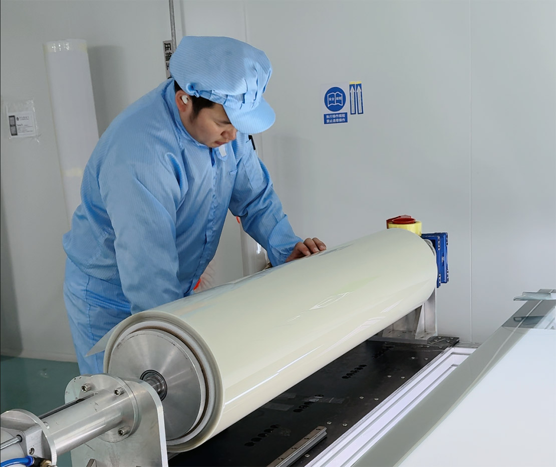
B): Nano-scale slurry coating
Slit coating + vacuum drying:
Gsnfilm Use a micro-gravure coating head (accuracy ±0.5μm) to coat PDLC slurry in a vacuum environment (pressure ≤50kPa) to avoid bubble mixing. The coating thickness is controlled at 20±0.5μm, and the surface density deviation is ≤1.5%.
Gradient temperature pre-curing:
Temperature control in three stages (40℃→60℃→80℃, 10 minutes each) to gradually volatilize the solvent (such as cyclohexanone) and form a stress-free liquid crystal-polymer precursor structure.
III. Vacuum lamination and UV curing upgrade
A): Vacuum hot pressing lamination
Dual chamber vacuum laminator:
The first layer (lower electrode + PDLC layer) and the second layer (upper electrode + protective layer) are preheated in a double-station vacuum chamber (80℃, 5 minutes), and then laminated through a precision alignment system (accuracy ±5μm), and finally pressurized for 30 minutes under **0.01MPa vacuum degree + 120℃** to ensure that there are no micro bubbles between the layers.
B): UV curing system upgrade
Pulse UV curing:
Gsnfilm Using LED-UV pulse light source (peak light intensity > 20W/cm², wavelength 365±5nm), irradiation time 50~100ms, instant curing, avoiding polarization drift of liquid crystal due to long-term heating.
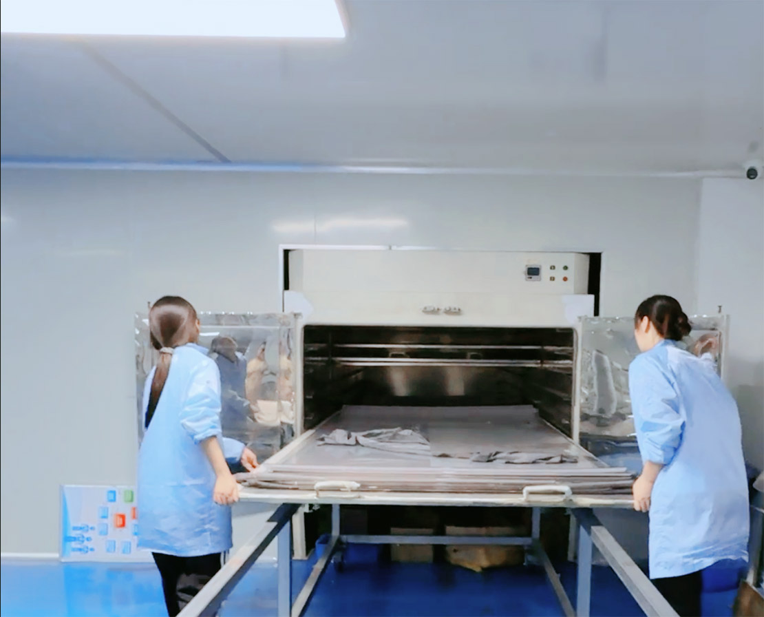
Nitrogen protection curing environment:
High-purity nitrogen (purity 99.999%) is introduced into the curing chamber, and the oxygen content is <10ppm, which inhibits the oxidation and yellowing of the polymer and ensures that the long-term transmittance attenuation is <3% (the attenuation of ordinary products is about 8%).
IV. Precision post-processing and strict testing
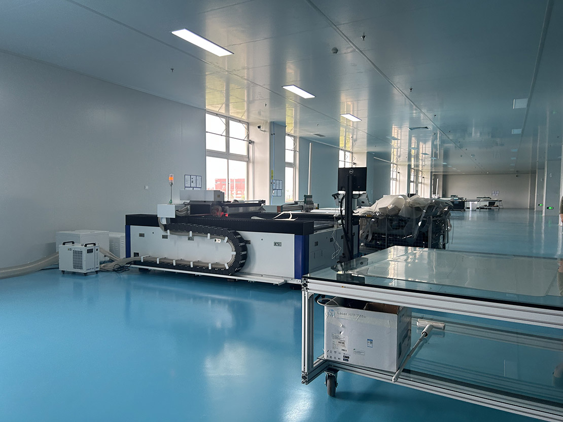
A): Laser cutting and edge sealing
Picosecond laser cutting:
Gsnfilm Using ultra-short pulse laser (pulse width <10ps) to cut the film material, the edge heat-affected zone is <10μm, avoiding edge delamination caused by traditional mechanical cutting.
Nano coating edge sealing:
The silicon dioxide (SiO₂) coating is deposited on the edge by vapor deposition (CVD) process with a thickness of 200~500nm to form a moisture-proof and oxygen-proof "molecular-level sealing layer". The performance retention rate after the heat and humidity test (85℃/85% RH, 1000 hours) is >95%.
B): Full process optical inspection
Laser speckle detection:
The film surface is irradiated with a 635nm laser beam, and the speckle pattern is captured by a CCD camera. The AI algorithm analyzes the uniformity of the liquid crystal droplet distribution, and the maximum droplet size deviation is allowed to be <5%.
Dynamic response test:
In a -40℃~85℃ temperature box, a high-speed camera (frame rate 1000fps) is used to record the atomization-transparent switching time of the power-on/power-off process, and the response speed fluctuation in the whole temperature range is required to be ≤10%.
Life Accelerated Test:
The xenon lamp aging test chamber (irradiance 1.2kW/m², cycle 120 minutes) was used to simulate a 10-year outdoor environment. After the test, the transmittance decay was <5% and the haze change was <2%.
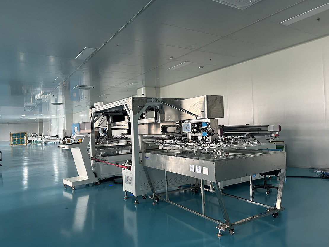
V. Intelligent Production and Traceability System
A): Digital Production Line
Equipped with MES system to monitor the parameters of each process (such as coating thickness, curing light intensity, lamination pressure) in real time, with a data acquisition frequency of 10 times/second. In case of abnormality, it will automatically trigger shutdown and trace the first 100 meters of products.
Visual Inspection Robot:
Equipped with a linear array CCD camera (resolution 1200dpi) and a deep learning algorithm, it can achieve 100% surface defect detection (minimum recognition size 0.1mm), and the rejection rate is ≤0.05%.
B): Key Technology Breakthrough Points
Molecular-level uniformity control: Through nanomaterial dispersion technology and vacuum process, the particle size distribution of liquid crystal droplets is concentrated in 2~3μm (4~6μm for ordinary products), and the optical scattering efficiency is increased by 30%.
Wide temperature range stability: Through fluorinated liquid crystal and high temperature resistant polymer, the optical performance fluctuation in the full temperature range of -40℃~85℃ is less than 5% (the fluctuation of ordinary products is about 15%).
Ability to resist extreme environments: After 100kPa high-pressure water washing and salt spray corrosion (5% NaCl, 1000 hours) tests, the resistance change of the conductive layer is less than 3%, and the interlayer adhesion retention rate is greater than 98%.
Gsnfilm not only relies on equipment precision and material innovation, but also ensures process stability through the Six Sigma quality management system (DPPM≤50) and ISO 14644-1 Class 5 clean workshop (dust particles ≤3520/m³, ≥0.5μm). This is why GsnfilmFilm can be applied for scenes with extremely high safety and reliability requirements.

LiveChatclose

 Send Email